
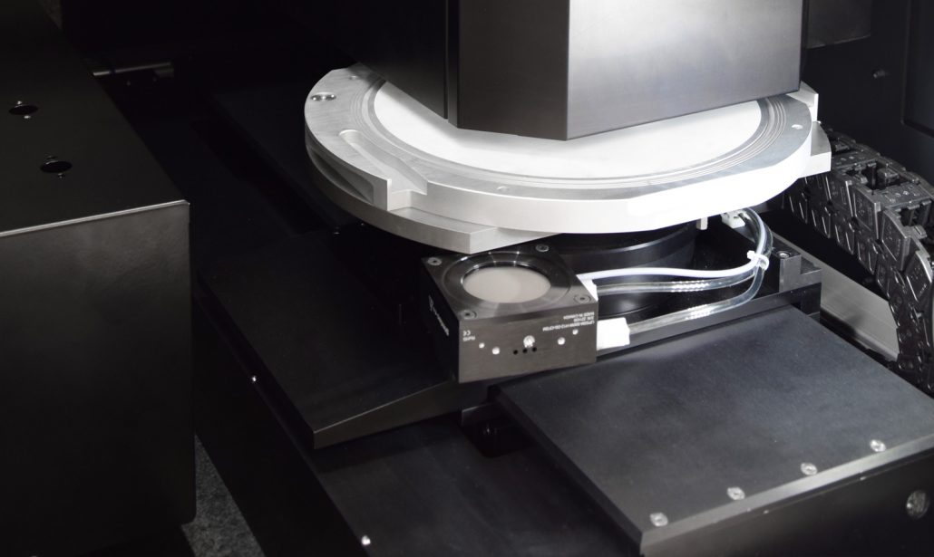
 The process of wafer dicing is used to separate die and a semiconductor after the wafer has been processed. The dicing process is accomplished by breaking and scribing. This is done with a laser or through mechanical sawing, during which a dicing saw is typically used. Each method is automated to help ensure accuracy and precision.
If the dicing process is followed, each of the chips created will be encapsulated into a chip carrier, which can then be used for building various electronic devices, such as computers. Keep reading to learn more about the process used for silicon wafer dicing…
 Though it is one of the most common causes of damage and destruction of property, a residential or business fire is often preventable. At the very least, there are typically some simple steps people can take to limit the amount of losses incurred if a blaze should break out inside a location or in the surrounding area. Keep the following tips in mind when considering how to increase your property’s fire safety protocol.