
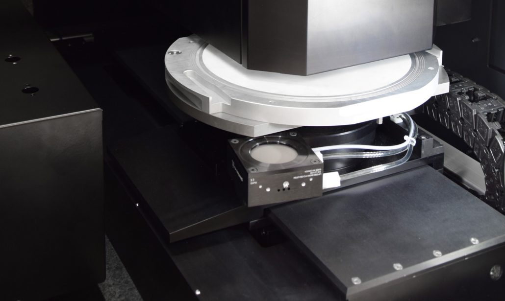
 The process of wafer dicing is used to separate die and a semiconductor after the wafer has been processed. The dicing process is accomplished by breaking and scribing. This is done with a laser or through mechanical sawing, during which a dicing saw is typically used. Each method is automated to help ensure accuracy and precision.
If the dicing process is followed, each of the chips created will be encapsulated into a chip carrier, which can then be used for building various electronic devices, such as computers. Keep reading to learn more about the process used for silicon wafer dicing.
The Dicing Process
During the dicing process, wafers will be mounted on dicing tape. This tape has a sticky back that will hold the wafer still on a thin frame made of sheet metal. There are several dicing tape options, each with different properties that depend on the particular dicing application. For example, UV curable tapes will be used for smaller sizes and the non-UV dicing tap is used for bigger die sizes.
After the wafer is dice, the pieces that remain on the dicing tape are called the dies, dice, or die. Each of these is packaged with proper packaging or they are put onto a printed circuit board substrate in the “bare die” form. The area that is cut away is referred to as die streets, which are usually around 0.0003 inches wide. After the wafer is diced, the die is going to remain on the dicing tape until they have been extracted by the handling equipment, such as the die sorter or die bonder, which happens later in the electronics assembly process.
An Essential Component of Electronic Assembly
While it may sound and seem complicated, this is a fairly common process that is used during the creation of various electronic components. Understanding how it works is essential for understanding this industry.